In 2021, IBM announced the introduction of 2 nm chip. It was a big break through as it proves Moore’s law again and is pushing the semiconductor industry to make smaller chips. And this is not the first time that “Xnm” makes headlines in Semiconductor Industry & Electronics Journal, but a similar trend happened when the first immersion and extreme ultraviolet lithography machine appeared. Because the industry was stuck for some time and not clear about its future roadmap.
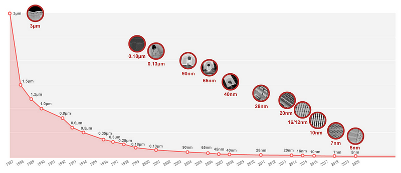
How does nm scale is getting smaller and smaller in the chip industry?
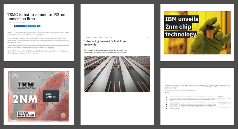
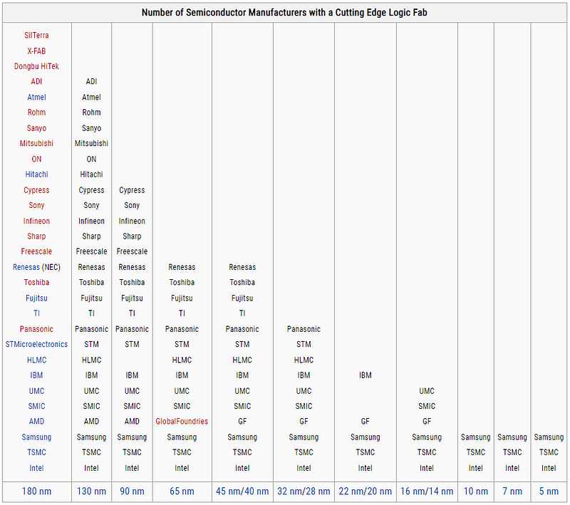
Source: TSMC
Basics:
Transistors, which act as a digital switch, are an intrinsic part of any chip. These transistors in the chip are wired together to function. In each Transistor, electricity flows from Source to Drain and is controlled by the gate (which is in between Source and Drain). And this length of gate is represented in nm, which we all hear in news like IBM creates first 2 nm chip. This is also termed as process node (also technology node) which refers to semiconductor manufacturing process rules. To avoid confusion, wavelength of light source is also measured in nm scale & is used in chip manufacturing, but that is not in headlines.
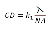
Lithography machines are mainly built on Rayleigh Criterion principle.
Rayleigh Criterion
Critical Dimension (CD), the size of a feature (which is exposed on the wafer to be part of the Chip), depends mostly on both lambda (wavelength of light source) and numerical aperture (NA-which capture light source). k1 is coefficient & its physical limit is 0.25. Smaller wavelength and higher numerical aperture makes size of feature smaller and sharper.
In the semiconductor industry, lithography machines are broadly divided into five major variants based on Rayleigh Criterion in last three decade. This classification is in general to process and not specific to lithography manufacturing companies.
1: Before DUV Litho Machine
~30–40 years back, lithography machines used light sources of wavelength 450 nm and 365 nm respectively. Then, wavelengths of light sources in lithography systems were 248 nm (krypton fluoride laser) and NA was in the range 0.65 to 0.80.
The wafer size (i.e, diameter of a wafer) used to be 200 mm (and less), although not part of Rayleigh Criterion principle but key factor to yield more dies.
2: DUV Dry Litho Machine
In early 2000, a lithography manufacturer started using a light source which was below the wavelength of light and known as deep ultraviolet (DUV). The DUV light source wavelength is 193 nm (argon fluoride laser) and NA is 0.93 (which was best at that time). Wafer size improved to 300 mm from 200 mm to fabricate more number of dies and cost-reduction on high volume manufacturing.
3: Immersion Litho Machine
In this variant, a light source travels through a lens, water and then reaches a wafer to print patterns. With this method, NA is scaled up to 1.35 from 0.93 but the wavelength of the light source is 193 nm. This is used to pattern sub-critical layers of the chip.
4: EUV Litho Machine
With the introduction of extreme ultraviolet (EUV) lithography, the wavelength of light sources is getting smaller by ~14 times, almost x-ray range. The EUV light source wavelength is 13.5 nm and NA is 0.33. This is used to pattern critical layers of the chip.
5: After EUV Litho Machine
This is known as the next version of EUV machines. In this variant, NA is scaled up to 0.55 from 0.33 and the wavelength is the same as EUV machine’s light source. These machines are expected to come into production by 2025 in Fabs for production of 3 nm or lesser size chips.
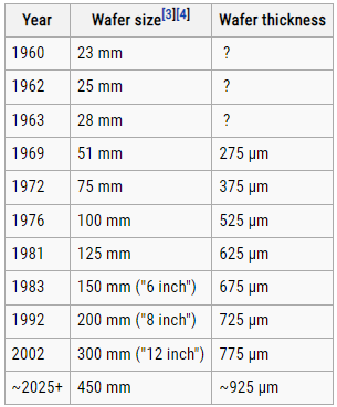
Wafer Size over time
During this “nm” journey (from ~450 nm to 5 nm or less), many companies went obsolete or at least not manufacturing the latest & smallest chip. Because for one company to accommodate the above changes like light source and NA, it needs huge investment with time. Many a time, it is a make-or-break situation. This holds true for both semiconductor Fab and lithography manufacturers.
Some companies (like IBM, Apple etc.) like to focus more on Design and Research of chip instead of manufacturing it. Other companies (like AMD) completely stopped semiconductor manufacturing and started to focus only on their design. Also, some semiconductor manufacturer use other leading manufacturer’s chip in their Soc.
Source: Wikichip
In lithography manufacturing, there were six players like SVG, GSA, Ultratech, Canon, Nikon, and ASML. Canon didn’t enter the immersion market. Only Nikon and ASML manufacture immersion systems. Now, only ASML manufactures EUV systems after three decades of research and acquiring lithography light sources company etc.
You might like to read a high level overview of Semiconductor industry here.


Leave a comment