In the digital era, Semiconductor devices are everywhere in some form or other, starting from mobile phones, automotive, healthcare, entertainment devices like play stations and etc. New Tech Domains like 5G, AI, IOT, self-driving Auto, Augmented Reality demand next-generation processors to solve complex calculations.
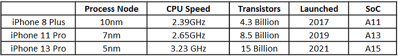
Next-generation processors usually come with smaller process nodes (i.e., the size of the smallest objects that the facility is capable of etching into the wafers). In 1990, the size of process nodes was bigger than 600 nm in 1990, and now it is 5 nm in the latest mobile phones. Recently IBM announced a chip with a 2 nm process node which will be extremely faster and increase the battery life by 4 times. But it will take time to hit the market because chips with 5 nm process nodes have just been rolled out in the latest mobile phones, but it was announced back in 2017.
Let’s explore the nm game, process & players.
How small is nm (i.e. nanometer)?
The thickness of A4 paper = ~75000 nm = 7.5e-5 meter
The diameter of human hair = ~50000–100000 nm = 5.0e-5–10.0e-5 meter
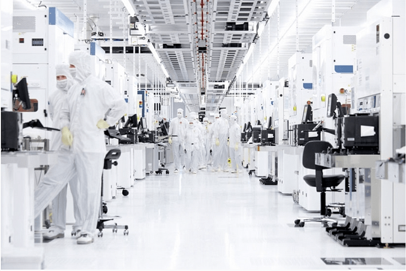
A nanometer is one-billionth of a meter, i.e. 1e-9 meter, which is ~10e–5 times smaller than human hair width. To avoid the smallest dust particles which can cause contamination in the manufacturing process, foundries comply with ISO standard class 5 or lower, so known as the one of the cleanest rooms on earth. The air in the foundries is filtered to 1000 times fewer airbone particles than in a sterile hospital operation room.
Also, manufacturing units for reticles are cleaner than foundries as reticle is a master chip design pattern that is used as a mask to print design on wafers in 4X or 5X reduction stepper in the fabrication exposure step.
What is the benefit of a smaller process node?
Transistors are the basic building block of any chip. Transistors act as digital switches to control the flow of electricity with states like On (i.e., binary value 1) and Off (i.e., binary value 0). It is essential because computers understand only binary values. Just recall The Matrix Collection movie.

Smaller process nodes increase transistor density, which gives the below benefits:-
- More transistors result in more calculations. Better performance.
- Electrons don’t have to travel a lot in smaller transistors, which reduces power consumption & becomes more power efficient.
- It leads to less faulty chips. Increases chip Yield.
Note: 1GHz = 1⁰⁹ Hz = 1⁰⁹ operations per second.
Also, Apple claims the new SoCs consume ~15% less battery life compared to the previous one. For example, A13 has better battery life than A12 and previous one.
How to make a smaller process node?
The photolithography process uses light sources and masks (i.e. reticles) to expose minutely thin patterns on wafers, and the type of machine mainly depends on the type of UV light used in this process.
Deep UV machines use wavelengths of 248–193nm. The next versions of DUV machines, i.e. Immersion DUV, use highly purified water as liquid between lens and wafer surface, unlike previous ones which use air, to create smaller process nodes.
Shorter wavelengths are used in the chip fabrication process to create smaller process nodes. The latest Extreme UV machines use EUV light of 13.5 nm wavelength to produce chips with process nodes ≤7 nm. This wavelength is more than 14 times shorter than DUV light.
An Immersion DUV machine costs more than half the cost of an EUV machine, but still provides better throughput than an EUV machine. Demand for DUV machines will not decrease as chip has different layers which need combination of different lithography machines. Most critical layers use an EUV machine, while critical layers use immersion and top layers use dry lithography machines.
Which companies are involved in this process?
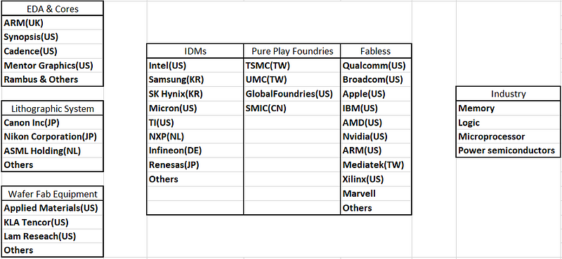
The semiconductor manufacturing process is incredibly complex and expensive. Latest Tesla factory in Germany created in ~1.5yrs with $5 billion, but to make a fab to manufacture semiconductor chips, it is required $10–20 billion & minimum 3yrs of time. CapEx Ratio required for fabs is 30–50% while only 3–5% for designers. Also, Fabless companies like to focus more on designing chips and outsource manufacturing processes to pure play foundries. Pure Play Foundries focus only on manufacturing chips for others. TSMC is the leading foundry with more than 50% market share with 500 clients worldwide. Integrated Device Manufacturers (IDMs) handle manufacturing both for in-house requirements and clients.
Only two companies (i.e. Nikon and ASML) manufacture wet immersion DUV machines, while ASML is the only manufacturer of EUV machines. Also, only two companies (i.e. TSMC & Samsung) are currently using EUV machines in their latest fab/foundries to produce ICs.
Which all industries need a chip?
Industry which provides better and safer (with precision) consumer experience by automating and optimizing the process, needs a chip.
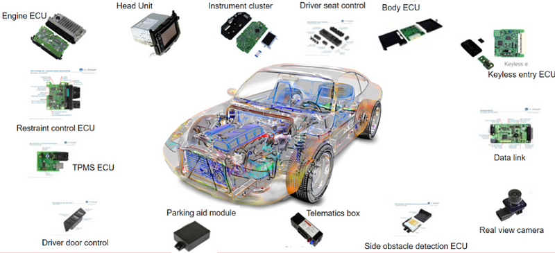
For example: automotive Industry. Most automotives use ECUs (Electronic control units), DCUs (which controls child lock, automatic windows, mirrors movement etc.), HMI (Human Machine Interface), sensors, ignition etc.
In the early years of air-bag deployment, car manufacturers thought 40-50 milliseconds were sufficient to avoid an accident. But accidents still happened and tests showed 50 milliseconds fine for 15mph and 18 milliseconds of deployment time was required for 35mph speeds. And this new deployment time can’t be achieved by electromechanical switches. Instead, they started to use ECUs and algorithms.
Latest EVs and self-driving cars use more chips (~ 1500+) for new features than current automobiles (~300 no. of chips). According to Koean news sources, Samsung Electronics will manufacture 5 nm chips for Tesla self-driving cars using EUV lithography machines.
Another example of improved consumer experience: listening to music. We did use audio cassettes some decades ago. Then we started listening on television, then laptop, then mobile phone. Then with smartphones, we started streaming using online tools, then using voice-to-text search on mobile phones. It is the same activity but with a huge difference in customer experience over decades.
What are the different steps in chip fabrication?
Broadly, there are around twelve fabrication steps which repeat 40–100 times depending upon the number of overlays for a chip design in a fab. Below are some of those steps :-
Slicing, Polishing, Deposition, Photoresist Coating, Exposure, Etching, Ion implementation, Photoresist Stripping, Test & Dice, Packaging.
Companies, who supply Wafer fab equipment, mostly deal with the above steps in foundries except exposure where lithography manufacturing companies are involved. Every company associated with this whole process, has an important role in creating chips which then are used in the end products like mobile phones, playstations, ECUs, data centers, Medical devices, automobiles, vacuum cleaners (cleaning robots), microwave, washing machine, wearable devices, cryptocurrency and many more.
Information mentioned here for the semiconductor industry is like the tip of the iceberg, but hope it will help to get an overview of the ecosystem. To know how process node is getting smaller & smaller, check here.


Leave a comment